Characterization CLA

optical microscope with camera

Responsibility:

SEM for inspection

FEI SEM, Nova NanoSEM 450

  • Magnification: 30x to 500,000x
  • Electron Gun: FEG with ultra-high brightness Schottky field emitter
  • Extracting Voltage (Vext): 0 to 5 kV
  • Acceleration Voltage (Vacc): 200 V to 30 kV (in deceleration mode: down to 50 V possible)
  • Lens mode: default: field-free, advanced option: immersion mode for ultra-high resolution imaging
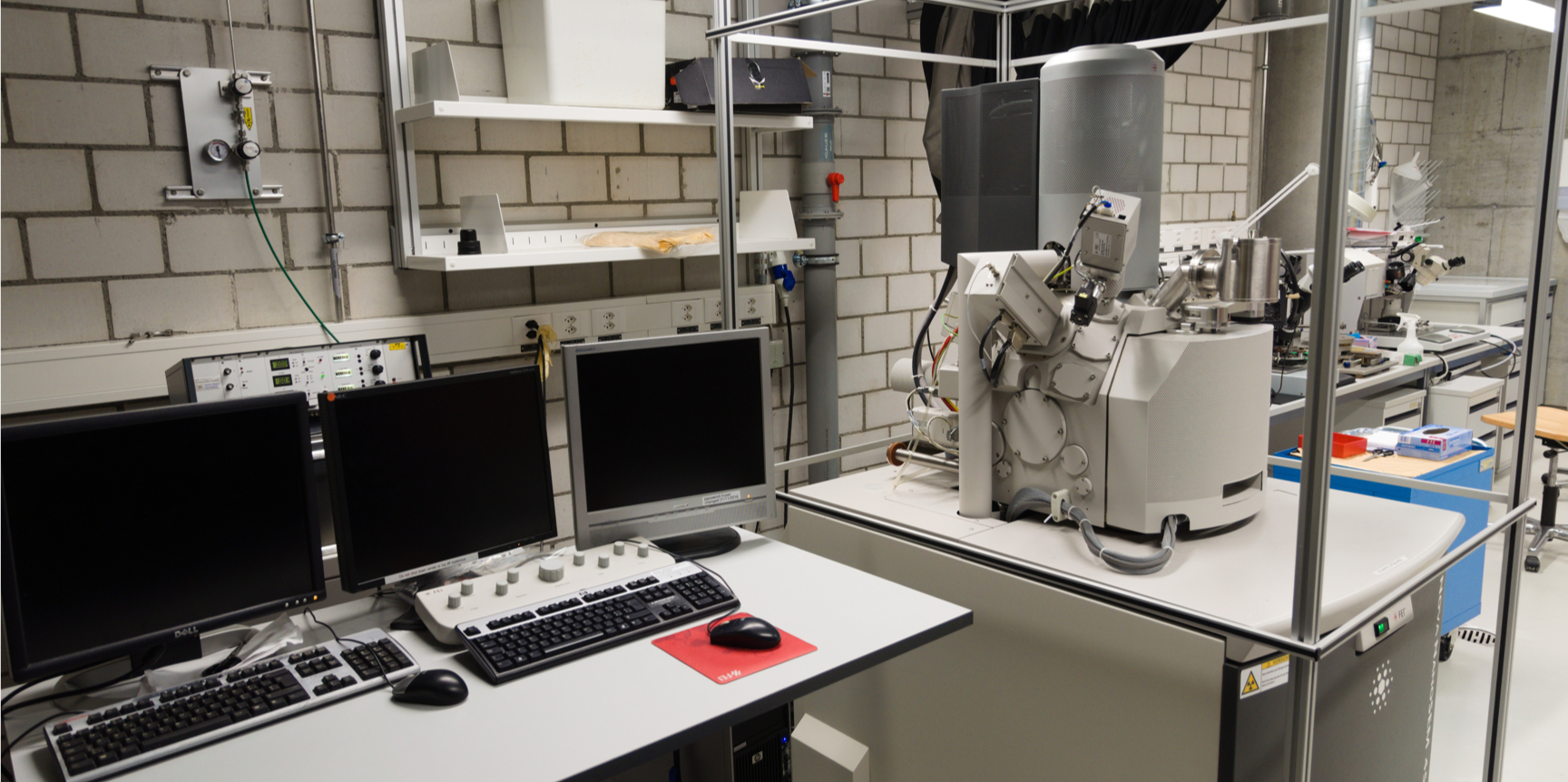
  • Detectors: ETD (default detector for field-free mode), TLD (default detector for immersion mode), detection of secondary electrons (SE) and back scattered electrons (BSE) possible
  • Chamber: Al with motorized 150 x 150 mm high precision and high stability stage and in-chamber camera
  • Stage: All 5 axes fully motorized, tiltable, possibility to mount up to 4 samples (e.g. 2 by 2 cm) or wafer
  • Vacuum: high vacuum operation (default mode)

Responsibility:


VTD Micro CT Scanner

Basic characteristics CT scan:

  • 3D X-ray computed tomography scanner
  • Dual source: 160 kV and 230 kV
  • High resolution: 4um (230 kV) and 0.4 µm (160 kV)
  • Inspection area up to 650 x 520 mm
  • Possibility to perform in-situ tests
  • Different scanning modes: conventional (2D and 3D), helical, laminography, shift and stack
  • Reconstruction and inspection software with artifacts correction algorithms

Responsibility:

Dektak XT surface profiler


  • Surface profiler for step height measurements
  • Vertical range 1 mm
  • Vertical resolution 1 nm
  • Scan length 55mm (150 mm with stitching)
  • Fully motorized
  • 3D mapping functionality

Responsibility:


White light interferometer

White light interferometer, Zygo NewView 5022s

  • General purpose 3D surface analyzer
  • Vertical resolution: 0.1 nm
  • Lateral resolution: 0.64 µm (@50X mag.)
  • Image zoom: 0.4X to 2.0X
  • Objectives: 5X, 20X, 50X
  • Image stitching for larger area mapping
JavaScript has been disabled in your browser