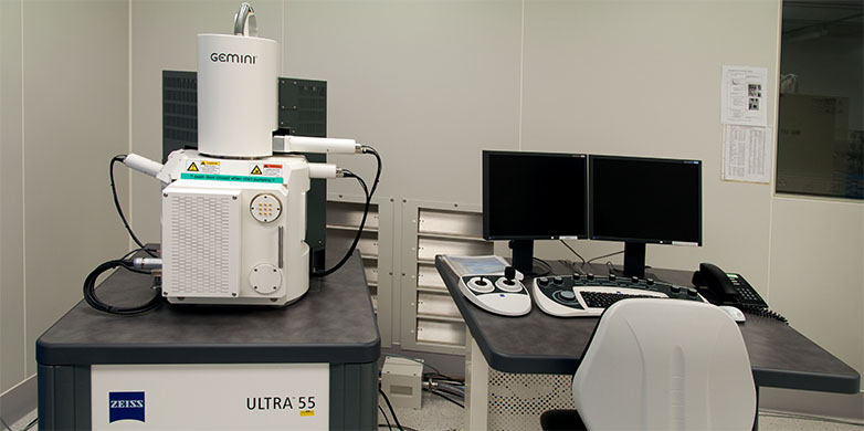
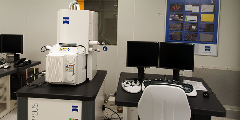
Scanning Electron Microscopy (SEM)

Please note that our equipment is dedicated to cleanroom processing only. For SEM measurements not requiring a cleanroom environment, please contact the Scientific Center for Optical and Electron Microscopy.

Responsibility:

Zeiss ULTRA 55:    


Zeiss ULTRA plus:   


Scanning electron microscope Zeiss Ultra 55
  • Digital Field Emission Scanning Electron Microscope
  • 0.1-30 keV beam energy
  • 1 - 1.7 nm resolution
  • ZEISS Complete Detection System with ET, Inlens SE, EsB and AsB detectors
  • Sample holders for chips, 2” and 4” substrates
  • All 5 axes full motorized
  • TIFF, BMP and JPG image up to 3072 x 2304 pixel resolution
Scanning electron microscope Zeiss Ultra plus

Zeiss ULTRA plus with integrated charge compensation

  • Digital Field Emission Scanning Electron Microscope
  • 0.02 - 30 keV beam energy
  • 1.7 nm resolution
  • ZEISS detection system with Inlens SE, EsB and SE detectors
  • Sample holders for chips, 2” and 4” substrates
  • All 5 axes fully motorized
  • TIFF, BMP and JPG image up to 3072 x 2304 pixel resolution
  • AVI – Image capture software for recording of audiovisual interleaves
  • Charge compensation: For isolating materials: resist, sapphire, glass, capton etc.
  • OptiProbe: Software system to adjust the probe current continuously

Responsibility:


Sputter system Pt (EM ACE200)

  • Sputter coating of non-conductive SEM samples with Pt, PdAu or Au
  • Ar plasma
  • 3 different targets available: Pt, PdAu or Au
  • Samples up to 4” diameter
JavaScript has been disabled in your browser