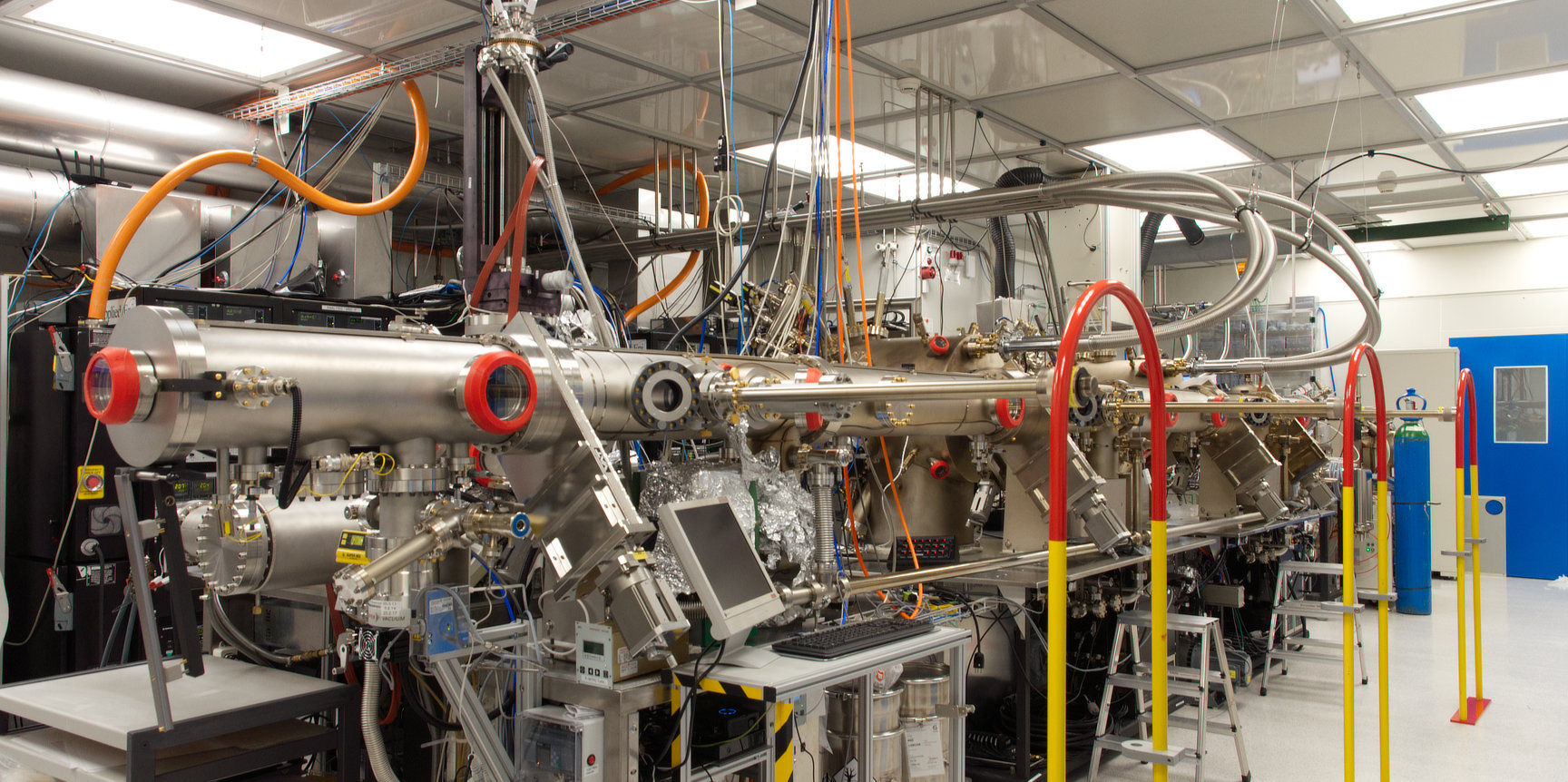
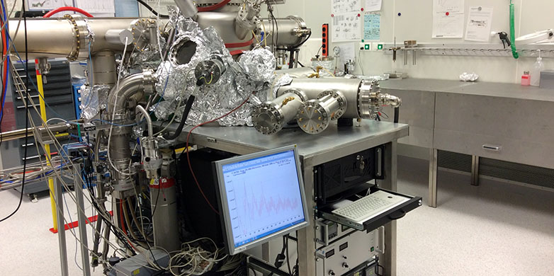
Substrate temperature monitoring using BandiT (band-edge thermometry).
Responsibility:
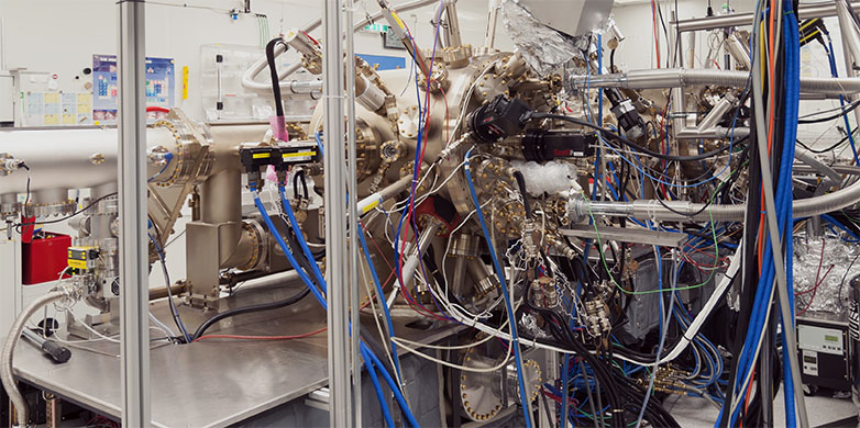
BandiT As-MBE
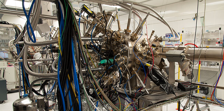
BandiT P-MBE
Optical temperature measurement of substrate surfaces.
Wet bench for cleaning and etching of UHV (Ultra High Vacuum) parts (MBE parts only)
Work bench for cleaning and working on UHV (Ultra High Vacuum) parts (MBE parts only)
Flow box for preparing holders and wafers (MBE only)
Circulating air oven for drying UHV (Ultra High Vaccum) parts (MBE only)