Optical Reflectometry

Metricon 2010/M Prism Coupler

Responsibility:


Metricon

The Metricon is a prism coupler to measure refractive indices and thicknesses. [1–3]

  • Rapid measurement ≤ 25 s
  • Thickness accuracy ±(0.5 % + 5 nm)
  • Refractive index/birefringence accuracy (±0.0005)
  • For low refractive indices films (≤ 3.5) and of bulk materials
  • Five different wavelengths (405 nm, 520 nm, 635 nm, 980 nm, 1550 nm). No advanced knowledge of optical properties of film/substrate is required.
  • Substrate size: 1 cm square up to 8'' square can be measured.
  • Substrate has to be polished
  • Attention: During the measurement, the sample is in direct contact with the prism over an area of 8 mm diameter.

Possible applications and materials:  

For organic/inorganic thin film and diffused optical waveguides rapid location of modes and automatic calculation of effective mode indices is possible. An inverse WKB calculation of index vs depth for graded index waveguides such as lithium niobate or ion exchanged glass can be done.

In-plane and perpendicular plane index for polymer materials can be measured permitting extremely simple and rapid determination of sample crystallinity and orientation.

Films on higher index substrates (such as silicon, GaAs, or other semiconductors) are not true waveguides, but fully accurate measurements of thickness and index can still be made on the leaky modes which result. Moreover, measurements of films on metallic or metal coated substrates are straightforward and are insensitive to the surface properties of the metal (i.e. smoothness/reflectivity) and thickness limits and performance are virtually indistinguishable from measurements on silicon.

Every step (baking, radiation exposure, etching) in the processing of polymer films causes changes in film thickness and index. Due to independent thickness and index measurements and unparalleled index resolution, the consistency of polymer and index anisotropy can be investigated. Furthermore, also nanoparticle/polymer films can be investigated.

If the upper film index is greater than that of the lower film, in many cases thickness and index may be measured for each film in a dual film structure (or for the first two films in a multilayer stack).

(Please double-check that your material is also allowed in FIRST)

Films: SiO2 (doped and undoped), silicon nitride, plasma SiN, silicon oxynitride, photoresists, polyimides, polyanyline, liquid crystals, PMMA, holographic gels, sol gels, silicon, SiC, diamond, epi garnets, electro-optic polymers, AlGaAs, BaTiO3, GaN, InP, ITO, KTP, MgO, PZT, PLZT, Si, Ta2O5, TiO2,YIG, ZnS, ZnSe, ZnCdSe, ZnMnTe, ZnMgTe.

Bulk materials: Quartz, optical glasses, chalcogenide glasses, sapphire, PET, polycarbonate, polyethylene, polystyrene, LiNbO3, LiTaO3, SiC, ZnS, GaP, GGG, MgO, YAG and other laser crystal

Substrate materials: Silicon, GaAs, glass, quartz, sapphire, GGG and lithium niobat

Basic prism coupling references:

  1. P. K. Tien, R. Ulrich, and R. J. Martin
    “Modes of propagating light waves in thin depositied semiconbductor films”
    Appl. Phys. Lett., vol. 14, no. 9, pp. 291–294, May 1969.
  2. P. K. Tien
    “Light Waves in Thin Films and Integrated Optics”
    Appl. Opt., vol. 10, no. 11, pp. 2395–2413, 1971.
  3. R. Ulrich and R. Torge
    "Measurement of Thin Film Parameters with a Prism Coupler,”
    Appl. Opt., vol. 12, no. 12, pp. 2901–2908, 1973.

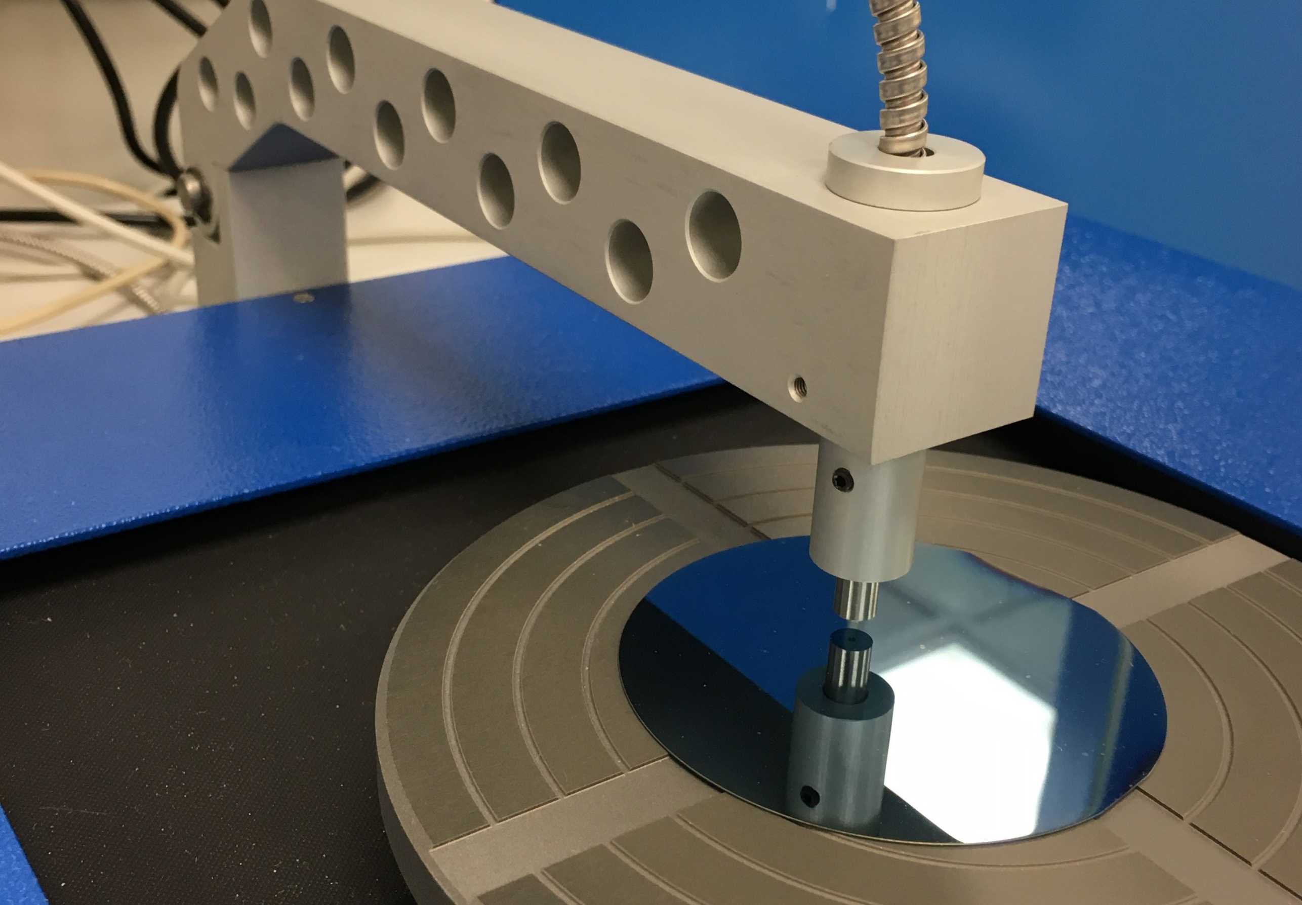
Optical reflectometer (Ocean optics)

Reflectometer

Responsibility:

  • Wavelength range: 270 nm - 1700 nm.
  • Mapping option.
  • Thickness analysis for samples with up to 10 thin films.
  • Sample size: wafers up to 6 inch in diameter.
  • Reference samples: Si, Al.
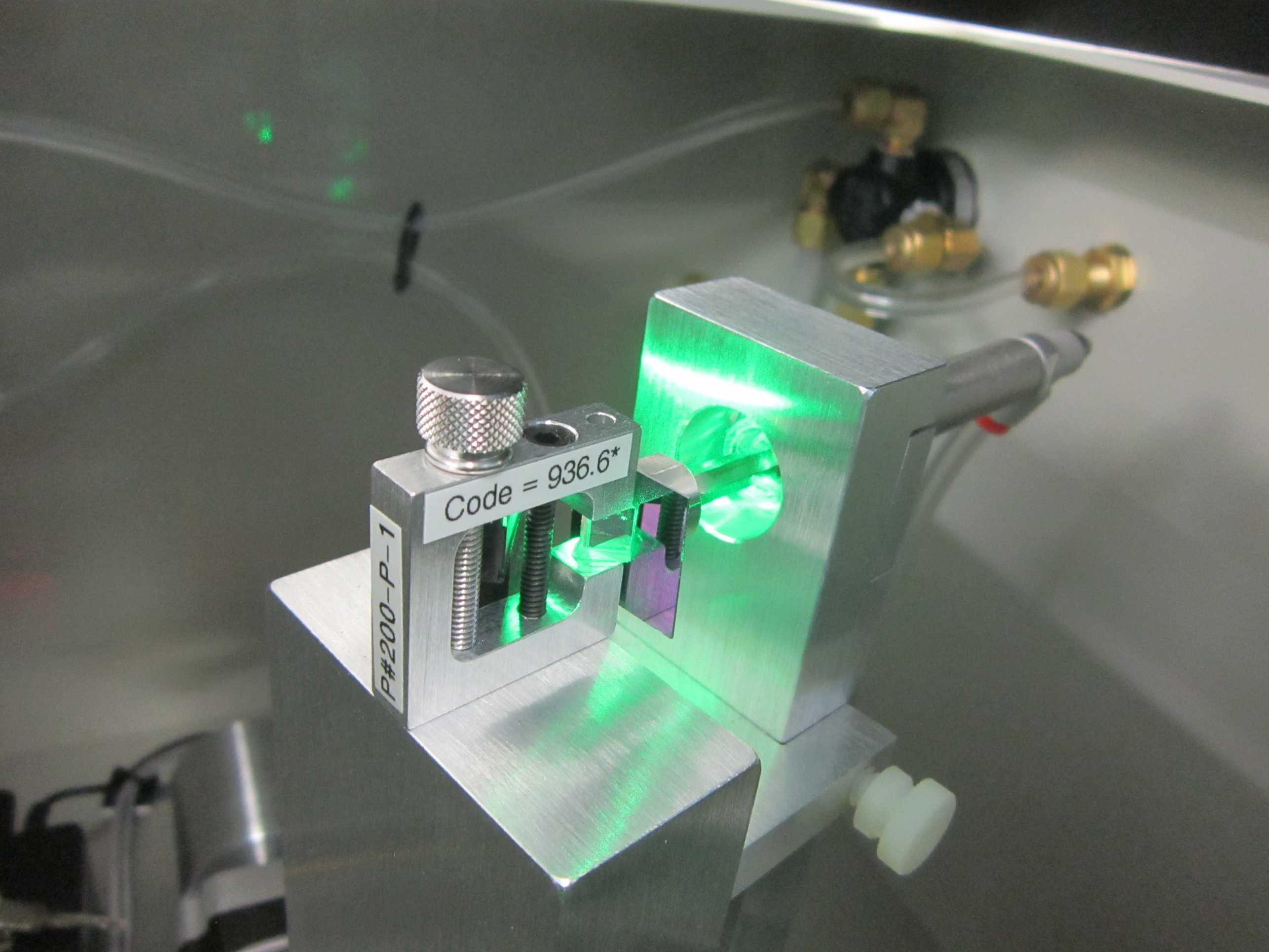
JavaScript has been disabled in your browser